A Software based DDS for 137Kc
By Dieter Wulff, DK5PT.
A short description of an experimental DDS
- Preface
This DDS-development should not be a competitor to the readily available DDS systems and ICs from ANALOG -DEVICES et. al.
The goal was to develop a cheap, amateur solution. After tests and experience with a DDS, made of discrete HC-MOS circuits which filled a complete lab-pcb. The idea was to replace the glue-logic by software.
- A bit of DDS-theory
The main components of a DDS or numerical oscillator, NCO, are:
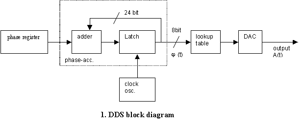
- the phase register
- the phase accumulator
- A clock oscillator
- lookup table
- DAC
The phase register holds the value of the phase increments. Every clock cycle this value is added to the preceding one. The result is latched and fed back to the binary adder.
The greater the value in the phase register, the faster the DDS steps through the signal phase, the higher the frequency. A complete phase cycle is finished, when the phase acc. rolls over.
To generate the output signal A(t), the linear phase information j(t) has to be converted to a harmonic signal. The lookup table holds the corresponding amplitude info. To generate A(t), the DAC is fed with the output of the lookup-table. The binary phase info is truncated to 8 bits in our example.
The table can hold sine info or other waveforms.
If the output of the phase acc. is fed directly to the DAC, a saw-tooth waveform with high harmonic contents would be the result.
The output frequency can be calculated with the:
DDS tuning equation:
 (equ. 1)
Where M is the value in the phase register (frequency set), n is the bit length of phase accumulator.
The frequency resolution of the DDS is:
 (equ. 2)
It depends only upon the bit-length of the phase acc. and the clock frequency.
Harmonics and spurs
The output of a NCO does not generate a continuous harmonic signal. Like many digital systems, the output signal is sampled in discrete steps (staircase function). To recover the output signal, an interpolation filter is needed.
In the frequency domain sampling generates harmonics of the sampling clock fclock, with the corresponding side-bands of the output frequency. In our LF narrow-band application, the harmonics can be filtered by a low-pass or band-pass filter.
Unfortunately frequency components can fold back into the desired output spectrum. These spurs are mainly a result of phase truncation and cannot be filtered . The amplitude quantisation adds noise to the signal. Math freaks can try to evaluate these frequency components by Fourier analysis of the “error voltage”, which is the difference between the wanted sin-voltage and the staircase approximation.
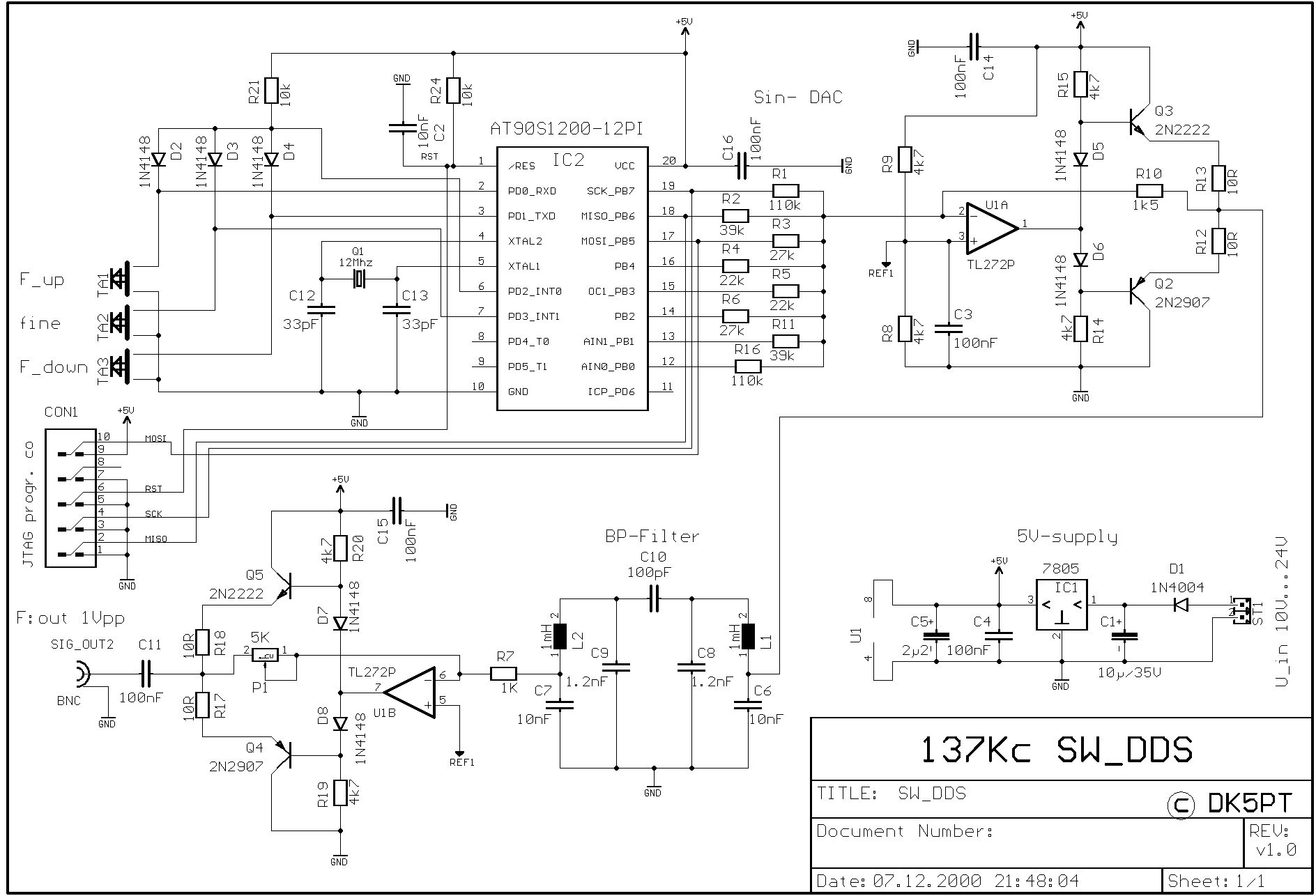
Circuit details:
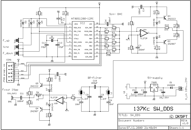
Click here for a full-size version
- µController
The AT90S1200 belongs to a new generation of low cost high speed RISC controllers manufactured by ATMEL.
These controllers can perform a single instruction within 80nsec (12Mc crystal).
They contain 32 internal registers, RAM and EEPROM and are in-circuit programmable via a JTAG connection. Programming SW can be downloaded from the ATMEL homepage.
A STK200 starter kit is available for programming the AT90xxxx controlers; Price in DL is abt 75,-eu.
- Software DDS
The AT90S1200 generates the samples of the desired output signal. The “software” main loop increments the 24 bit phase accumulator, transforms the (linear) phase information j(t) to a binary output word BW(t) via a look up table.
The complete software-loop needs 10 instructions, so the sampling frequency fclock is 1.2Mc. About 8.7 samples of the desired output frequency fout are generated.
The BW (t) is output via port PB0….PB7 to a “Sin- DAC”, which converts the binary data directly to a Sin-output current. The following current to voltage converter , IC U1a, delivers the final harmonic signal u(t) to a band-pass filter.
A buffer amplifier completes the circuit with a low impedance voltage source. The output voltage can be adjusted to 1V RMS.
Tuning is performed simply: Three pushbuttons are used to increase or decrease the output frequency. -The middle button allows smaller f-steps. All buttons are “ored” to the interrupt input, because the software main loop cannot poll the buttons. If the buttons are down, an auto increment funktion is activated. The interrupts of the auto increment are audible.
Pushing both outer buttons simultaneously will reset the frequency to a default value of abt137kc. Referring to equ.2, a theor. frequency resolution of about 0.07cy is possible, but not realized. The “coarse” tuning increments in abt. 20cy steps, “fine” tuning is done in 5 cy steps. Both can be changed by software, if necessary.
It should be mentioned, that the “absolute” accuracy is of minor importance; The quartz used, is a cheap µC-type, with about 10-5 precision. For higher accuracy, an external Qu-oscillator should be used.
- The Sin DAC
Converting binary data to a signal in the time domain can be done in many ways. Mostly common are DACs with a binary weighted resistor network, i.e. a R-2R network. These DACs produce a 2n amplitude resolution. The disadvantage is the high accuracy needed for the resistors and the resulting glitches, which occur when more than one bit switches simultaneously.
The kind of DAC used for the DDS is a “thermometer” type. The binary output of the AT90S1200 is comparable to a shift register, where a binary “ones” followed by a binary “zeros” are shifted through all outputs.
The R network is “Sine” weighted. - it can be built of simple 1%- E96 series resistors.-
Every new increment of the phase acc. produces an equivalent (non-linear) current step, which approximates the Sin with a “staircase” function.
This are 16 steps in the realised circuit.
Finally the staircase function (samples) are smoothed by means of an interpolation (reconstruction) filter which is designed as a137kc high Q band-pass.
- Measurements
Most of the time has been spent on measuring the spurs and harmonics. Tests on 274kc, showed a worst case spurious free dynamic range (SFDR) of 34dB, too bad in my opinion.
It is too close to the Nyquist frequency , which is Fclock/2=600kc. The SFDR is degraded in this region.
The same procedure at 137kc increased the worst case SFDR to about 46dB, which is not bad for such a simple system. All measured with a selective VOM, a time consuming job.
The SFDR behaviour is strongly dependent on the used frequency, and is difficult to predict. One frequency step can alter the SFDR from 46dB to more than 60dB! The BP-Filter has a strong influence on the achieved SFDR and the harmonics.
- Experimental realisation
The circuit is completely assembled on a lab-PCB. (see picture). The PCB size is 10cm x 6cm. It fits into a small shielded box. The 5V regulator is mounted on a side wall. Total current consumption is 30mA.
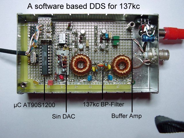
High Q 1mh toroids, or ferrite coils should be used for the design of the bandpass recovery filter.
The ATMEL AT90S1200-µController is a DIP 20 type; The 12Mc- high speed version must be used!
The OP-amp used for the I/U converter is a cheap dual FET-type TLC 272 (DIP8); Unity gain bandwith is abt 2Mc. It works with a single 5V supply.
The complementary transistors are small signal types; Others, like the BC547/BC557, can be used as well.
This project is not for “beginners” on LF. Expirience in rf- and test gear is required.
Dieter , DK5PT
Ordering special parts
|
Part |
Manufacturer |
Farnell order code |
apprx. price “Euro” |
|
AT90S1200-12PC |
ATMEL |
690752 |
5.30 |
|
TLC272P |
Texas |
401158 |
1.0 |
|
Coil 1mH 8RB type |
Toko |
148143 |
0.8 |
Download the hex code and diagram.
The files: DDS12V10.hex ( the hex-program file for the AT90S1200 controller ) , SW-DDS1.gif ( the full sized circuit diagram ) and SW-DDS.doc ( the text ) can be downloaded as a 68k Zip file: dk5ptdds.zip.
E-mail Dieter at
Return to features index.